Chinese Researchers Achieve 100x AI Inference Speed Boost with All-Optical Chip Interconnect Using One-Ninth the Computing Power
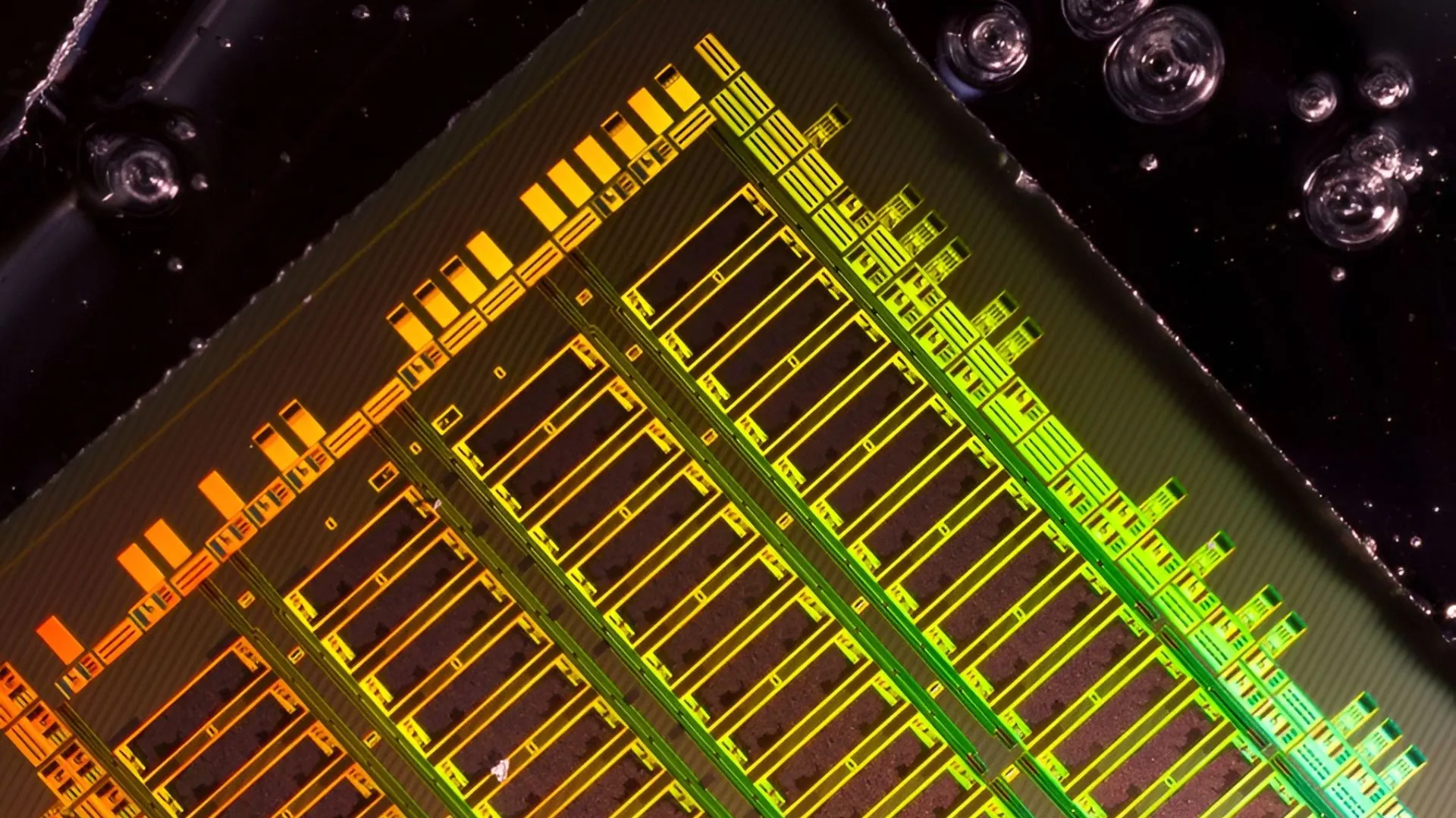
A Peking University research team has developed an all-optical interconnect system that accelerates distributed AI inference by more than 100 times while consuming only about one-ninth the computing resources of conventional GPU systems. The prototype features a 400 Gbps silicon photonic transceiver and a 16×16 optical switching chip, delivering a total switching bandwidth of 6.4 Tbps. The findings have been published in National Science Review.
Highlights
- Peking University's all-optical interconnect prototype delivers over 100x faster AI inference compared to a commercial GPU, using only one-ninth of its computing resources.
- The system's core components are a 400 Gbps silicon photonic transceiver and a custom 16×16 optical switching chip, providing a total switching bandwidth of 6.4 Tbps.
- The optical switch achieves a total insertion loss of less than 5 dB, enabling error-free, high-speed transmission without external optical gain compensation.
- A five-layer CNN for image denoising was used to validate the architecture, with feature maps transmitted directly through the optical network to eliminate memory transfer latency.
- The findings were published in National Science Review, with researchers highlighting the system's potential to reduce data center energy consumption and support edge AI deployments.
Chinese Researchers Achieve 100x AI Inference Speed Boost with All-Optical Chip Interconnect
A research team at Peking University has developed an all-optical interconnect system capable of dramatically accelerating distributed AI inference performance while requiring only a fraction of the computing resources demanded by conventional GPU-based setups. The prototype demonstrated inference speeds more than 100 times faster than a commercial GPU system, using approximately one-ninth of its computing resources.
The system connects multiple computing chips via an on-chip all-optical network, replacing traditional electrical wiring. The design aims to reduce latency and improve inter-chip data transfer efficiency — addressing a bottleneck that becomes increasingly pronounced as AI workloads continue to scale.
At the heart of the system is a 400 Gbps silicon photonic transceiver that converts electronic signals into optical signals and back. It works in tandem with a custom 16×16 optical switching chip that routes data between computing nodes, forming a scalable communication network with a total switching bandwidth of 6.4 Tbps.
The researchers say this design shifts the focus from simply adding more compute hardware to improving how chips communicate, enabling multiple processors to collaborate more efficiently during AI inference.
Replacing the Bottleneck with Light
A key characteristic of the optical switch is its total insertion loss — including coupling loss — of less than 5 dB. According to the team, this enables high-speed, error-free transmission without requiring external optical gain compensation. The switch also maintains error-free performance across multiple communication paths and supports a spectral response range exceeding 100 nm, making it compatible with future bandwidth expansion via wavelength-division multiplexing (WDM).
To validate the architecture, the researchers deployed a five-layer convolutional neural network (CNN) for an image denoising task. Each layer was assigned to a separate computing unit, with the optical switch linking the processors into a pipeline.
Rather than repeatedly writing intermediate data to memory before passing it to the next processor, the system transmits feature maps directly through the optical network. This significantly reduces memory transfer latency and keeps each computing unit in continuous operation.
Compared with a commercial GPU performing the same image denoising task, the optical system delivered more than 100 times the inference speed while requiring approximately one-ninth of the computing resources.
A Different Path to Scaling AI
The researchers argue that their work points to an alternative route for improving AI performance as models continue to grow.
"When algorithms, processor microarchitecture, and chip-level interconnects are co-designed, specific goals can be achieved under constrained computational resources," the paper's authors wrote.
"This architecture can also alleviate unsustainable energy consumption in data centers and optimize latency or power consumption for edge computing scenarios," they added.
The team noted that advances in co-packaged optics, silicon photonic transceivers, and faster AI chip interfaces could turn on-chip optical supernodes into practical building blocks for future distributed computing systems. Such systems would offer high bandwidth, low latency, and strong energy efficiency to support next-generation AI workloads — without relying solely on ever-larger, increasingly power-hungry processor clusters.
The research has been published in National Science Review.
原文來源: 查看原文
FAQ
Newsletter
Subscribe to our Low-Altitude Industry Newsletter
Daily curated news on low-altitude economy and drone industry, delivered to your inbox.
Reviewed and published by the LAETimes editorial desk ·